- 您现在的位置:买卖IC网 > Sheet目录3862 > PIC18F45J11-I/ML (Microchip Technology)IC PIC MCU FLASH 32K 2V 44-QFN
2010 Microchip Technology Inc.
DS70138G-page 209
dsPIC30F3014/4013
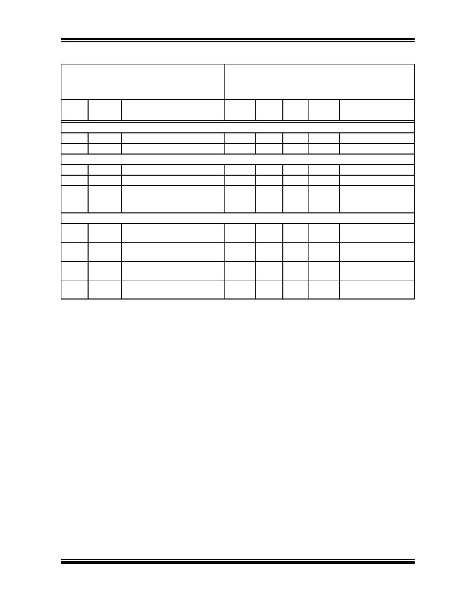
TABLE 23-38: 12-BIT A/D CONVERSION TIMING REQUIREMENTS
AC CHARACTERISTICS
Standard Operating Conditions: 2.7V to 5.5V
(unless otherwise stated)
Operating temperature
-40°C
TA +85°C for Industrial
-40°C
TA +125°C for Extended
Param
No.
Symbol
Characteristic
Min.
Typ
Max.
Units
Conditions
Clock Parameters
AD50
TAD
A/D Clock Period
334
—
ns
VDD = 3-5.5V (Note 1)
AD51
tRC
A/D Internal RC Oscillator Period
1.2
1.5
1.8
s
Conversion Rate
AD55
tCONV
Conversion Time
—
14 TAD
ns
AD56
FCNV
Throughput Rate
—
200
—
ksps
VDD = VREF = 5V
AD57
TSAMP
Sampling Time
1 TAD
——
ns
VDD = 3-5.5V source
resistance
RS = 0-2.5 k
Timing Parameters
AD60
tPCS
Conversion Start from Sample
Trigger
—1 TAD
—ns
AD61
tPSS
Sample Start from Setting
Sample (SAMP) Bit
0.5 TAD
—1.5
TAD
ns
AD62
tCSS
Conversion Completion to
Sample Start (ASAM = 1)
—0.5 TAD
—ns
AD63
tDPU(2)
Time to Stabilize Analog Stage
from A/D Off to A/D On
——
20
s
Note 1:
Because the sample caps will eventually lose charge, clock rates below 10 kHz can affect linearity
performance, especially at elevated temperatures.
2:
tDPU is the time required for the ADC module to stabilize when it is turned on (ADCON1<ADON> = 1).
During this time the ADC result is indeterminate.
发布紧急采购,3分钟左右您将得到回复。
相关PDF资料
SFW15R-2STE1
SFW15R-2STE1-FFC/FPC CONN
PIC18F26J11-I/ML
IC PIC MCU FLASH 64K 2V 28-QFN
PIC18F46K20-E/ML
IC PIC MCU FLASH 32KX16 44QFN
PIC24FJ64GA002-I/SO
IC PIC MCU FLASH 64KB 28SOIC
PIC16C711-04/P
IC MCU OTP 1KX14 A/D 18DIP
PIC18LF26K22-I/SP
IC PIC MCU 64KB FLASH 28SPDIP
PIC18F25K80-I/SP
MCU PIC 32KB FLASH 28SDIP
DSPIC33FJ12MC201-I/SS
IC DSPIC MCU/DSP 12K 20SSOP
相关代理商/技术参数
PIC18F45J11-I/PT
功能描述:8位微控制器 -MCU 32KB Flash 4KBRAM 12MIPS nanoWatt RoHS:否 制造商:Silicon Labs 核心:8051 处理器系列:C8051F39x 数据总线宽度:8 bit 最大时钟频率:50 MHz 程序存储器大小:16 KB 数据 RAM 大小:1 KB 片上 ADC:Yes 工作电源电压:1.8 V to 3.6 V 工作温度范围:- 40 C to + 105 C 封装 / 箱体:QFN-20 安装风格:SMD/SMT
PIC18F45J11T-I/ML
功能描述:8位微控制器 -MCU 32KB Flash 4KBRAM 12MIPS nanoWatt RoHS:否 制造商:Silicon Labs 核心:8051 处理器系列:C8051F39x 数据总线宽度:8 bit 最大时钟频率:50 MHz 程序存储器大小:16 KB 数据 RAM 大小:1 KB 片上 ADC:Yes 工作电源电压:1.8 V to 3.6 V 工作温度范围:- 40 C to + 105 C 封装 / 箱体:QFN-20 安装风格:SMD/SMT
PIC18F45J11T-I/PT
功能描述:8位微控制器 -MCU 32KB Flash 4KBRAM 12MIPS nanoWatt RoHS:否 制造商:Silicon Labs 核心:8051 处理器系列:C8051F39x 数据总线宽度:8 bit 最大时钟频率:50 MHz 程序存储器大小:16 KB 数据 RAM 大小:1 KB 片上 ADC:Yes 工作电源电压:1.8 V to 3.6 V 工作温度范围:- 40 C to + 105 C 封装 / 箱体:QFN-20 安装风格:SMD/SMT
PIC18F45J50-I/ML
功能描述:8位微控制器 -MCU Full Spd USB 32KB 4KBRAM nanoWatt RoHS:否 制造商:Silicon Labs 核心:8051 处理器系列:C8051F39x 数据总线宽度:8 bit 最大时钟频率:50 MHz 程序存储器大小:16 KB 数据 RAM 大小:1 KB 片上 ADC:Yes 工作电源电压:1.8 V to 3.6 V 工作温度范围:- 40 C to + 105 C 封装 / 箱体:QFN-20 安装风格:SMD/SMT
PIC18F45J50-I/PT
功能描述:8位微控制器 -MCU Full Spd USB 32KB 4KBRAM nanoWatt
RoHS:否 制造商:Silicon Labs 核心:8051 处理器系列:C8051F39x 数据总线宽度:8 bit 最大时钟频率:50 MHz 程序存储器大小:16 KB 数据 RAM 大小:1 KB 片上 ADC:Yes 工作电源电压:1.8 V to 3.6 V 工作温度范围:- 40 C to + 105 C 封装 / 箱体:QFN-20 安装风格:SMD/SMT
PIC18F45J50T-I/ML
功能描述:8位微控制器 -MCU Full Spd USB 32KB 4KBRAM nanoWatt RoHS:否 制造商:Silicon Labs 核心:8051 处理器系列:C8051F39x 数据总线宽度:8 bit 最大时钟频率:50 MHz 程序存储器大小:16 KB 数据 RAM 大小:1 KB 片上 ADC:Yes 工作电源电压:1.8 V to 3.6 V 工作温度范围:- 40 C to + 105 C 封装 / 箱体:QFN-20 安装风格:SMD/SMT
PIC18F45J50T-I/PT
功能描述:8位微控制器 -MCU Full Spd USB 32KB 4KBRAM nanoWatt RoHS:否 制造商:Silicon Labs 核心:8051 处理器系列:C8051F39x 数据总线宽度:8 bit 最大时钟频率:50 MHz 程序存储器大小:16 KB 数据 RAM 大小:1 KB 片上 ADC:Yes 工作电源电压:1.8 V to 3.6 V 工作温度范围:- 40 C to + 105 C 封装 / 箱体:QFN-20 安装风格:SMD/SMT
PIC18F45K20-E/ML
功能描述:8位微控制器 -MCU 32KB Flash 1536B RAM 25 I/O 8B RoHS:否 制造商:Silicon Labs 核心:8051 处理器系列:C8051F39x 数据总线宽度:8 bit 最大时钟频率:50 MHz 程序存储器大小:16 KB 数据 RAM 大小:1 KB 片上 ADC:Yes 工作电源电压:1.8 V to 3.6 V 工作温度范围:- 40 C to + 105 C 封装 / 箱体:QFN-20 安装风格:SMD/SMT